
HDI PCB Manufacturer UK — High Density Interconnect Circuit Boards
PCB Company is a specialist HDI PCB manufacturer based in the UK, delivering high-density interconnect circuit boards to engineers, OEMs, and procurement teams across aerospace, medical, automotive, and telecommunications sectors.
As a division of RUSH PCB UK Ltd with over 20 years of experience, we manufacture HDI PCBs from 4 to 32 layers using advanced laser-drilled microvias, blind and buried vias, and sequential lamination technology.
If you are looking to reduce the size of an existing PCB design, route a fine-pitch BGA, or improve signal integrity for high-speed signals, our UK-based engineers will offer a free DFM review for every HDI PCB design.
What Is an HDI PCB?
According to IPC-2226, an HDI (High Density Interconnect) PCB is a printed circuit board that has a greater wiring density per unit area than traditional PCBs. Some of the technical characteristics that make up HDI boards are microvias that are 150µm or less, finer lines and spaces of ≤100µm, capture pads that are less than 400 µm, and more than 20 connection pads per cm².
Instead of mechanically drilled vias like you would see on a typical through-hole PCB, HDI PCBs use laser-drilled microvias and build-up lamination. The use of these two processes allows the component density to be much greater in a smaller area. Designers can decrease the total layer count (i.e., an 8-layer through-hole board could be converted to a 4-layer HDI board) without sacrificing electrical performance.
HDI is the overall board technology; laser-drilled microvias are one of the key interconnect methods used to build it. For detailed information on microvia drilling, blind and buried connections and fine-pitch routing, see our laser drill micro vias service.
Why Choose HDI PCB Technology?
HDI PCB UK makes high-density interconnect PCBs with various features such as impedance control, high-speed transmission capability, and low radiation. Consequently, our boards allow the use of miniature components because of the enhancement of wiring density. Moreover, customers can use leadless, fine-pitch components and direct chip bonding with our advanced PCB boards that feature exceptional high-density. Some advantages of the HDI board UK are:
- Firstly, High Density
- Fewer Layers
- Uses Miniature Components
- Uses Fine-Pitch Components
- Prominently, High-Speed and High-Frequency Operations
- Low Weight
- Lastly, Smaller Size
Our high-density interconnect PCBs bring innumerable benefits to our customers. Specifically, the HDI board UK offers high-speed and high-frequency operation in considerably smaller sizes as compared to regular boards. As the routing density is high, we can make high-density interconnect PCBs with fewer layers.
Furthermore, the low weight and small size of our HDI circuitry mean they can fit into smaller spaces, allowing the final product to also be lightweight and smaller. Consequently, a reduction in both parameters is an indication that the product will be less susceptible to mechanical shocks and vibrations.
Please explore our services, and we assure you the best from our side. Moreover, we offer our customers the best value and results for their boards, independent of the service you decide to use:
- PCB Prototype UK Services
- Quick Turn PCB UK Services
- PCB Manufacturer UK Services
- PCB Assembly UK Services

Who Uses HDI PCB UK?
Our HDI PCBs are widely used across the UK B2B sectors:
- Aerospace & Defence — Avionics, radar, satellite communications (high reliability Class 3).
- Medical Devices — Imaging systems, patient monitors, implantables.
- Automotive & EV — ADAS, LiDAR, power electronics, infotainment.
- Telecommunications & 5G — Base stations, routers, RF modules.
- Industrial Automation & IoT — Sensors, control systems, smart manufacturing.
Regardless of whatever your requirement for HDI circuits may be, we can give you the optimum solution. Simply mail us your Gerber files today.
Our PCB Prototype UK services are a great way for our customers to stick to their budget, while still obtaining the superb quality and services that PCB Company offers, on time and guaranteed.
Thus, with our PCB supplier UK services, our customers can keep track of their projects and get their boards just-in-time. If you require boards fast, take advantage of our flexible lead times of 1 to 21 days.
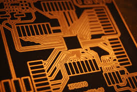
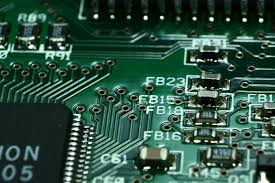
HDI PCB Fabrication
Our HDI PCB design UK comes with high-density features like laser-drilled micro-vias, high-performance fine copper traces, and high-performance thin substrate materials. Consequently, as the routing density is high, designers can achieve extra functions per unit area. Moreover, the high density and routing resolution are perfect for using large pin-count chips that mobile devices and other high technology products depend upon.
Our HDI PCB Manufacturing Process
As an HDI PCB manufacturer in the UK, we offer several types of services to our customers:
- Free DFM/DFA Review
- Inner layer imaging & etching with AOI
- Sequential lamination with precise dielectric control
- Laser drilling of microvias
- Electroless & electrolytic copper plating
- Fine-line outer layer processing (LDI)
- Surface finish application
- Electrical testing (flying probe, impedance)
- Final inspection & UK delivery
Our advanced PCB boards require special handling, like extra precision while mounting components, as they are denser than regular boards. Our customers can mount fine-pitch components, leadless components, and other miniature parts.

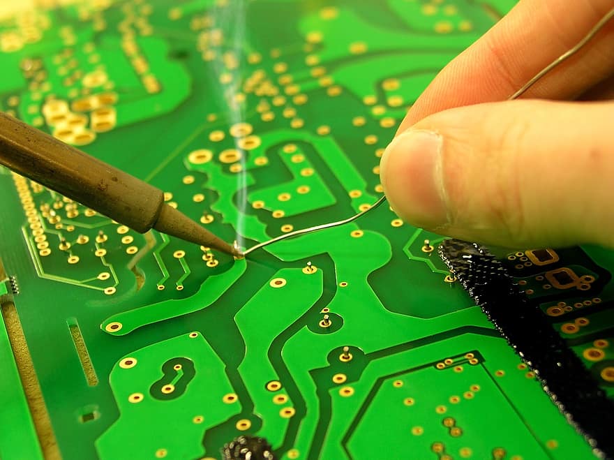
Surface Finish
As an HDI PCB manufacturer in the UK, PCB Company offers several types of surface finishes:
- HASL with Lead
- HASL without Lead
- Immersion Silver
- Immersion Gold (ENIG)
- Hard Gold
- Finally, OSP
In addition, we also offer several additional options for our boards. These include:
- Impedance Control
- Z-Axis Milling
- Half-Cut Holes
- Castellated Holes
- Countersunk Holes
- Counterbore Holes
- Buried Vias
- Blind Vias
- Stacked Vias
- Staggered Vias
- Laser Drilled Micro-Vias
- Via-in-Pad
- Via filled with Resin
- Via filled with Copper
Contact us for more information, and ask for a quotation while submitting your design files online. Further, we offer instant quotes. Try us today.
Why Choose an HDI PCB Manufacturer UK?
Our customers choose to use the HDI board UK for various reasons. PCB Company has:
- 10 years of experience
- A skilled team
- Statistical quality control
- PDCA processes
- Full surface treatment production processes
- Advanced machines for:
- Stack Up
- Automatic V-cut
- Laser drilling
- Mechanical drilling
- Automatic exposure
- Laser Direct Imaging
- Automated Optical Inspection
- Temperature cycling equipment
Another reason why our customers use our HDI PCB UK is that they are cost-effective while still maintaining the essential factor of high quality. For instance, we can effectively shrink an 8-layer through-hole board to a 4-layer HDI board packed with technology like laser-drilled micro-vias.
Additionally, we use state-of-the-art technology while building our boards, and this increases the cost of our HDI PCBs. However, our HDI PCB design reduces the layer count, thereby lowering the cost of materials. That makes boards from the HDI PCB manufacturer UK more cost-effective as compared to traditional boards.
FREQUENTLY ASKED QUESTIONS
The benefits of HDI PCBs include smaller and lighter electronic items, better performance in electricity usage, and increased capability to support high-speed and high-frequency signals. They also allow development of extremely fine-pitch, miniature components for more compact and complex designs.
The micro-via structure of laser-drilled HDI PCBs with fine copper traces is made with thin, high-performance substrate materials. These materials and processes yield a high density of routed board and electrical performance.
These PCBs combine many integrated circuits with fine pitch or micro-vias, so it’s needed to pay a lot of attention to the control of impedance, signal integrity, and heat flow within the board. Other important features are that some fabrication methods like laser drilling, should be employed to achieve densely packed interconnections or avoid other related problems.
The small dimensions and heights, coupled with great quality of performanc,e make HDI PCBs popular in almost all fields of consumer electronics like mobile phones, tablets, or wearable computer devices. They are also widely used in the aerospace, military, and medical industries, where dependability and miniaturization are needed.
For a quote, you may refer to the PCB Company’s website or give them a call. For the most precise quote in the shortest time, it is best to provide design files as Gerber files.