PCB Materials Choosing the appropriate printed circuit board material is crucial in today's world of…
02 Layer and 04 Layer: PCB Bare Boards
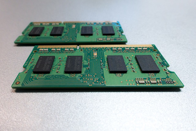
What are 02 Layer and 04 Layer PCBs?
02 Layer
On both sides of the printed circuit board, conductive copper and components can be mounted using a two-layer PCB, allowing the traces to cross over. Consequently, it results in a higher board density without the requirement for point-to-point soldering.
04 Layer
If a manufacturer is creating a 4-layer PCB, they will undoubtedly use one core, prepreg, and copper foil for the top and bottom layers. According to their construction, which consists of four copper layers fused, four layers of PCB may accommodate a high level of PCB complexity.
Additionally, PCB producers have started using a core made of the same material as a standard two-layer PCB. the layers keep together and transform into hard fiberglass when the board is heated in a press. As a result, four layers of PCBs are strong and resilient following the curing process.
The Stack-ups of 2 Layers PCBs and 4 layers PCBs
On the two layers of the PCB stack up, layer 1, or the top layer, is described as a signal layer. The copper layer, which is 0.0014 inches thick and weighs around 1 ounce, has a positive impact on the boards that are 0.062 inches thick, or roughly 10% of the total thickness.
Depending on the essential requirements, these values may change if your board is manufactured. On the other hand, a four-layer PCB stack is rather complicated because it includes the top and bottom layers in addition to the two inner levels, inner layers 1 and 2.
The prepreg layer, which has a thickness of 0.0091 inches and a dielectric constant of 4.2, is placed beneath the signal layer (0.0014 inches wide), which is the top layer of a four-layer PCB stack-up.
Copper material makes up the top layer. Inner layer 1, often known as the plane, follows the prepreg layer and is 0.0014 inches thick. Inner layer 1, which is 0.037 in wide, includes a core sublayer. Inner layer 2, a plane layer that is 0.0014 in. thick and made of 1 oz. copper comes next.
Two 0.0091-inch-thick sheets make up another prepreg sublayer, which is a portion of inner layer 2. The bottom layer, which is the final layer, is a signal layer as well and is 0.0014 inches thick. On the top and bottom layers, it solders and attaches the interconnects.
When should I choose 2 Layer PCBs or 4 Layer PCBs?
You must think about the requirements of your project and which type best matches them when deciding whether to use 2 layers of PCB or 4 layers of PCB. There are a few things you should know:
- What is the largest that a PCB can be? For 4 layers of PCB, there is more functionality in a smaller area.
- How much functionality do you mandate? You will require 4 layers of PCB if your project is more complicated.
- How about sturdiness? Select a
- layer PCB if exceptional durability is a must.
- How much is the budget? It is preferable to select two layers of PCB if your budget allows for it.
- How soon do you require your boards? Comparing 2 layers PCB to 4 layers PCB, the lead time is less.