PCB Materials Choosing the appropriate printed circuit board material is crucial in today's world of…
Solder Mask Expansion – Purpose and Working on a PCB
What is Solider Mask Expansion: Purpose and working?
The significant support to the initial pad/via shape to generate the desired solder mask layer shape. If you provide a positive value, the initial pad/via shape will expand; if you enter a negative value, it will shrink. It is the increased space between the solder mask layer and the SMT pads.
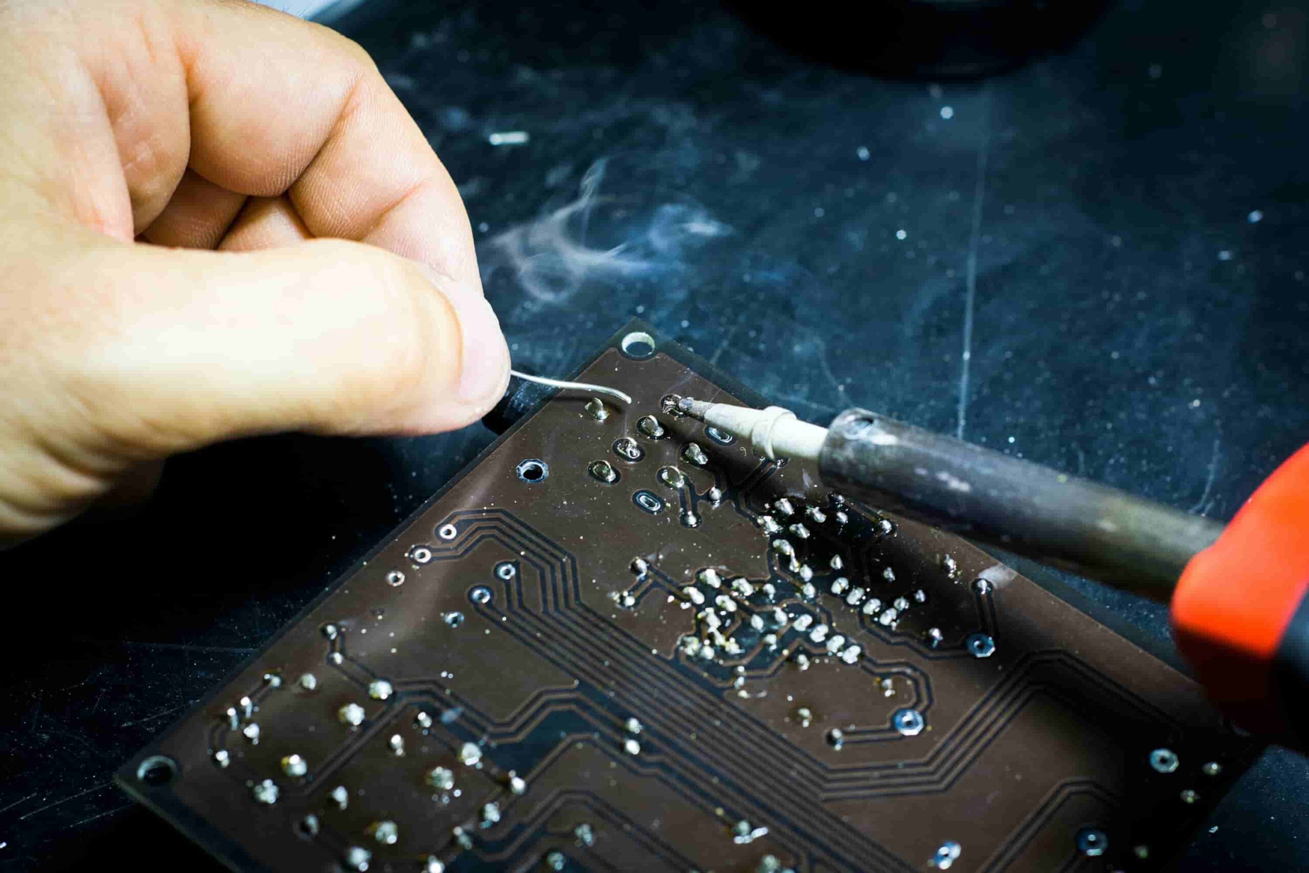
Pads on the solder mask layer should have some room during printed circuit board manufacture to prevent the solder mask layer and pads from touching. Solder masks should never be placed on top of SMD pads when designing PCBs.
The majority of PCB design software programs let you either generically (for the entire board) or individually specify the distance between the solder mask and surface parts (for elements).
Characteristics of Solder Mask Expansion
Another option is to specify both of these design characteristics and let the computer program use rules to decide which specification to use in each situation. The solder mask expansion is the name given to this parameter, which can be positive, zero, or negative.
- Positive Solder Mask Expansion: A distance between the pads outside the perimeter and the end of the solder mask surrounding it is said to have positive solder mask expansion.
- Zero Solder Mask Expansion: There is no “gap” or space between the end of the pad and the beginning of the solder mask with zero solder mask expansion.
- Negative Solder Mask Expansion: When the solder mask partially encloses the pad, negative solder mask expansion occurs. The value is the separation from the pad’s outer edge to where the solder mask ends.
Zero solder mask expansion would, in most situations, be desirable because it would provide the necessary solder dam and maximum board protection. Negative expansion, however, may be preferable in some circumstances, such as when tenting is used to cover a via to stop the solder from being sucked into the hole. Practically speaking, it is better to specify a positive or negative solder mask expansion that can be manufactured by your design requirements and is compatible with your CM’s equipment.
Solder Mask Expansion Limitations:
1. Choosing the proper value for the Expansion restriction will result in both partial and full tenting of pads and vias:
a. Set the Expansion to a negative value to close the mask up to the pad/via hole if you just want to partially tent a pad/via covering the land area.
b. Set the Expansion to a negative value equal to or greater than the pad/via radius to completely tent a pad/via, enclosing the surrounding area including the hole.
c. Set the proper Expansion value and confirm that the rule’s scope targets all pads and vias on the necessary layer to order to tent all pads and vias on a single layer.
d. Set the Expansion to a negative value equal to or greater than the maximum pad/via radius to completely tent all pads/vias in a design with defined varied pad/via sizes.
2. Pads and vias can each have their solder mask expansion configured in the related properties dialog. Users have the choice of adhering to the expansion provided in the relevant design rule or bypassing it and applying a particular expansion specifically to the specific pad or route in question. There are additional options to compel the pad or to completely tent on the top and/or bottom.
Contact: PCB Company Uk for more information